Current Process Parameters
Process Procedure
Photolithography is a process used in microfabrication to pattern parts in a thin film or the bulk of a substrate. A layer photoresist is applied to the wafer surface, then exposed to ultraviolet light through a photomask. After development, only selected area of the wafer will be covered with the photoresist, leaving the rest of the wafer open. This prepares the wafer for a subsequent etch step which requires certain regions of the wafer surface to be masked off.
The photolithography process consists of the following steps:
- DEHYDRATION
- SPIN COATING
- ALIGNMENT AND EXPOSURE
- DEVELOPMENT
- INSPECTION AND HARD BAKE
1. DEHYDRATION
Place a wafer in an aluminum dish keeping the front side up, and then place the Al dish into the Dehydration oven which is pre-heated to 120 °C. Keep the Al dish with the wafer in the oven at least 10 minutes. This step will completely dry wafer so any moisture on the wafer surface is baked out.
2. SPIN COATING
Remove the Al dish from the dehydration oven, and place the dish in an opaque polypropylene box, and move to a nitrogen blower. Then, using the nitrogen gun, blow the wafer surface to remove any dust particles. Note that keep the wafer in the Al dish during the blowing and blow only the side to be coated.
Bring the wafer in the box to the Spin Coater. Make sure that the program (or recipe) of the coater is set appropriately for the photoresist and application. Using Teflon tweezers, place the wafer on the wafer chuck in the center of the Spin Coater. After making sure the wafer is centered on the wafer chuck, apply 4 – 8 drops of primer (P-20) on the wafer with a liquid dropper. Then close the lid of the Spin Coater and press START button. This will allow promote good adhesion between the photoresist and the wafer surface. After the Spin Coater stops, a short pre-bake, e.g. 1 minute in a Pre-bake oven, can be applied to the substrate.
After the Spin Coater is fully stopped, photoresist can be applied to the wafer surface. A new liquid dropper should be used for applying photoresist to avoid particle contamination. After applying enough drops of photoresist to cover 70 – 80 % of the wafer surface, close the lid of the Spin Coater and press START button. This will allow even and uniform coating of the photoresist on the wafer. Note that the spinning speed and time needs to be checked based on the photoresist and target thickness. If the coated photoresist is defective or not uniform, ask the instructor for further options. After the Spin Coater completely stops and vacuum is released, use the Teflon tweezers to carefully remove the wafer and place it into the Al dish. In order to evaporate residual solvent from the coated photoresist film, the wafer is pre-baked (soft-baked) either in a Pre-bake oven or on a hot plate. For example, for the S1813 photoresist on 2-inch wafers, the wafer in an Al dish is baked for 5 minutes in the Pre-bake oven at 95 °C. Let the wafer cooled down in the box, then proceed to the alignment and exposure step.
3. ALIGNMENT AND EXPOSURE
The MA-6 mask aligner is used for aligning patterns and exposing photoresist with UV light. A photomask consists of a soda-lime glass (or quartz) substrate and a patterned metal layer on the substrate. The size of the photomask should be at least one inch larger than the wafer. For example, a 4- by 4-inch photomask is used for 2-inch wafers and a 5- by 5-inch photomask is for 4-inch wafers.
First, the intensity of UV light should be measured with the provided intensity meter. Place the sensor calibrated for the appropriate wavelength on the wafer plate of the aligner and then, press the LAMP TEST
button to start emission of the UV light. Read and record the light intensity and use it for determining the exposure time for the photoresist thickness you are using. Press LAMP TEST
again to turn off the light emission. The measurement of the intensity of UV light and the loading of the photomask are usually performed by the instructor in advance. Note that the UV lamp behind the aligner remains on always. Enter parameters such as exposure time and alignment gap in one of the Programs (Hard contact, Soft contact, and Vacuum contact) of the MA-6.
Press button CHANGE MASK
to start to load the photomask. Place the photomask on the mask holder, facing the metal side upward. Use the three extruded metal posts and a bottom clamp as guides to the proper position of the mask. Toggle the vacuum to ON
by pressing the ENTER
button. Carefully turn the mask holder upside down and slide it into the mask stage. Gently push holder up to top right corner and press the CHANGE MASK
button to fix the holder in the position. The metal side of the mask will face to the wafer side after proper loading.
Once the mask is loaded and secured, the photoresist-coated wafer can be loaded and exposed. Press the LOAD
button to load the wafer, then follow sequential instructions appeared on the green display of the machine. Make sure the coated side of the wafer is loaded upward and the wafer edge gently touches the three extruded screws on the wafer chuck when placing the wafer on the wafer chuck. Align the wafer to the mask by using the stage X, Y and θ (rotation) micrometers. Adjust position of the microscope with the arrow buttons if needed. Check the alignment by pressing the ALIGN CONT/EXP.
or the ALIGNMENT CHECK
buttons, which makes the wafer contact the mask using the contact mode you selected during setup. Pressing the button once again allows you to adjust the alignment if the alignment was poor. When the alignment is satisfactory, press the EXPOSURE
button to expose the wafer with the UV light for the programmed time. Wait until the machine give the instruction of UNLOAD THE EXPOSED WAFER,
then unload the wafer.
After unloading the wafer from the wafer chuck, push the wafer chuck back into the slide and re-center the stage indicator with the X, Y and θ micrometers. Then, proceed to the development step. A post-exposure bake step can be done before the development, if needed.
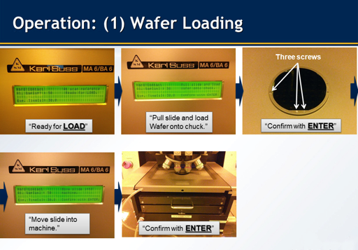 Wafer loading sequence
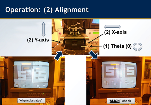 Alignment sequence
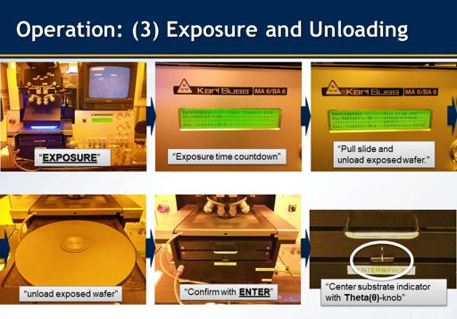 Exposure and unloading sequence
4. DEVELOPMENT
A developer solution is determined by the type of photoresist chosen. For example, MF-391 is a developer for S1813 photoresist and RD-6 for NR9-1500PY photoresist. As an example, the development procedure of a 2-inch wafer with S1813 photoresist is explained. Fill a Pyrex beaker about 2/3 full of the MF-319 developer while turning on the D.I. water supply in another beaker in the sink. Using Teflon tweezers, carefully place the wafer into a Teflon wafer holder and lock it up with a slider. Set a timer, then immerse the wafer in the developer for a given time. In this example, it takes 30 seconds. Then, immediately immerse the wafer into the other beaker under running D.I. water and rinse it for one minute. Move the wafer holder with the wafer to the drying station and blow the wafer and the holder using the N2 guns.
5. INSPECTION AND HARD BAKE
The wafer is inspected under a microscope to see whether the patterns are clear and well defined. The sharpness, dimensional accuracy, and clearness of the patterns can be checked during the inspection. If everything meets specifications and the process is required, the wafer is placed in the Hard Bake oven which is preheated to 120 °C for 10 minutes. The hard bake makes the resist more stable and hardened for subsequent physical or chemical processes.
If the inspection results are not good, the photoresist is stripped off by using 1165 remover or acetone. The wafer is dried using a nitrogen blower, and then re-work from the dehydration step.
(Back to top)