Current Process Parameters (Spring 2020)
Processing Equipment
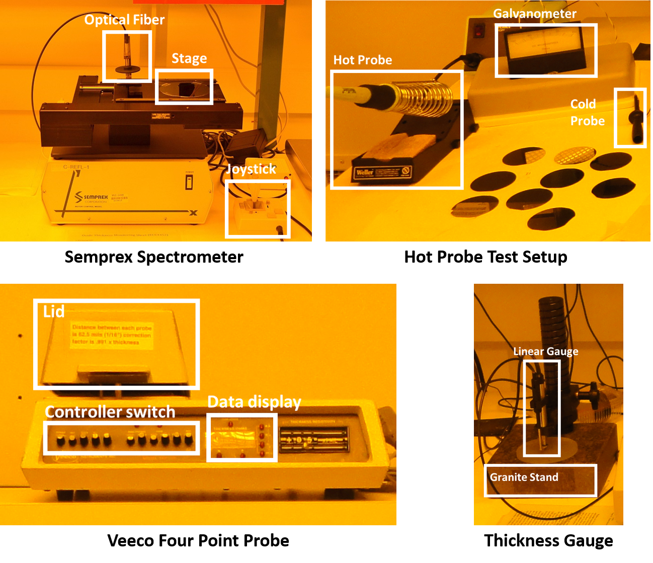 Metrology Equipment
Process Procedure
It is crucial to characterize silicon substrates and thin films in semiconductor fabrication processes. The substrate must be tested because the dopant type and concentration must be correct for the process to yield devices with the desired characteristics. Since doping concentrations and conductivities of the substrate changes from the processes of the semiconductor microfabrication, the characterization and measurement on the substrate should be conducted whenever they are affected. Thin film processes, including growth, deposition, and etching, also require measurement with appropriate methods to characterize the processes. Correct methods of characterizing substrates and films can monitor quality of processes and provide assurances about the result of processes.
In this procedure, featured methods for fundamental characterization of silicon substrates and thin films are described.
- CRYSTALLINE ORIENTATION
- HOT PROBE METHOD
- THICKNESS GAUGE
- FOUR POINT PROBE
- SPECTROMETER
1. CRYSTALLINE ORIENTATION
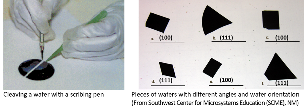
Wafers are grown from crystal having a regular crystal structure. Single crystalline silicon has a diamond cubic structure with a lattice spacing of 5.4 Å. When cut into wafers, the surface is aligned in one of several relative directions known as crystal orientation. Orientation is defined by the Millar Index, with (100) and (111) crystallographic orientations being the most common for integrated circuit fabrication. The orientation is important since many of single crystal’s structural and electronic properties are highly anisotropic. Wafer cleavage typically occurs only in a few well-defined directions.
To scribe a silicon wafer, start from the wafer flat on the wafer. Place the tip of a scribing pen at the center of the flat and snap through the edge of the wafer with the tip, gently but firmly. Repeat the snap at the same position until you see the wafer breaks into two half-circle pieces. Then, repeat the snap cleaving on the fresh-cut line of the piece. The second cut make the wafer pieces angled at either 90 ° or 60 °.
The orientation of the wafer surface plane breaks at 90 ° angles for (100) wafers, and 60 ° angles for (111) wafers. The example pictures of cleaved pieces of wafers are in below from the Southwest Center for Microsystems Education (SCME), NM.
 Wafer Crystalline Orientation
2. HOT PROBE METHOD
One of the properties of silicon is that it can be doped with impurities to become either N or P type. One way to determine whether the wafer is either N or P type is to place a hot probe, such as a soldering iron, and a cold probe on the wafer surface. Then, measure the direction of current flow between two probes using a galvanometer. If the current flow from the hot probe to the cold probe, the wafer is N-type. If it is P-type, the current flows in the opposite direction.
3. THICKNESS GAUGE
The wafer thickness can be measured using a thickness gauge. A Mitutoyo’s Granite Comparator Stand is mounted with a precision Linear Gage. Place the wafer on the base and lift the gauge by using a cable release. Gently lower the gauge to the wafer surface and read data from the indicator. Note that the units of the indicator are set in millimeters.
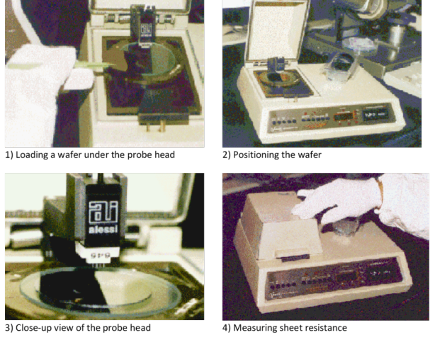
4. FOUR POINT PROBE
A Four Point Probe is to measure resistivities of any semiconductor material. It can measure either bulk or thin film specimen. The Four Point Probe consists of four equally spaced metal tips with a defined radius. Each tip is supported by springs on the other end to minimize sample damage during probing. The four metal tips are part of mechanical stage which travels up and down during measurements. A current source is used to supply current through the outer two probes while a voltmeter measures the voltage across the inner two probes to determine the sample resistivity. The Veeco Four Point Probe in the Instructional Cleanroom measures resistive properties of semiconductor wafers and resistive films. The microprocessor-based electronics permits direct computation of V/I, Sheet resistance, Resistivity and P-N type testing.
Place a wafer under the probe head and locate the position of the wafer where the sheet resistance is to be measured. Close the lid and gently press and hold. While the lid is closed, the sheet resistance is measured, and the value is displayed. Also, note the P-N type indicator. Open the lid and move to the next position of the wafer for further measurements.
 Four point probe measurement sequence
5. SPECTROMETER
In spectroscopic reflectometry, samples are illuminated with a white light, usually a deuterium halogen bulb or a tungsten halogen bulb, at an incident angle normal to the sample. Then the reflectance and interference from the sample surface are measured. Due to the nature of a thin film coating on a substrate, optical constant measurements at various wavelengths are required to obtain the right fit of the measured reflectance curve relative to the theoretical reflectance curve. A database of optical constants n and k is used to develop the theoretical reflectance curve for a given material on a specific substrate. The first step of the sampling process involves measurement of a reference substrate, i.e. a bare silicon wafer. This is followed by the sample measurement using the same conditions. Upon capturing the data, software algorithms are used to fit the measured data to theoretical calculated values derived from the database of optical constants. The software will calculate a thickness value based on this fit. The software will also generate a mean square error (MSE) to indicate how well it was able to fit the measured data to the theoretical data. The MSE will indicate how accurate the derived thickness is.
To operate the Semprex Spectrometer, turn on the connected laptop and wait for the software SPECTRUM SUITE
to open. Turn on the white light source and place a silicon wafer under the light. Click REF
on the menu and follow the instruction from the software. Remove the reference wafer and place the sample wafer with a thin film layer under the white light source. Use the joystick to position the stage at location you want to measure. Click START
to have the first measurement. Then move to the next positions and click GO
to collect the next measurements. A bar graph and a spreadsheet will show the measurements. In order to measure another sample, click QUIT
, load the new sample, and click START.
After finishing the measurement, turn off the light source and the laptop.
(Back to top)