The Instructional Cleanroom has capability of fabricating integrated circuits on silicon wafers, including MOSFETs, diodes, resistors, and capacitors. The equipment in the Instructional Cleanroom supports all the required processes to fabricate these microelectronic devices, including oxidation, diffusion, photolithography, metallization, and etching. The equipment can process various sizes of silicon substrates from small pieces up to 4 inches. Thus, fully functional MOSFETs and diodes can be fabricated in the cleanroom.
The CMOS fabrication capability is used to teach graduate and senior undergraduate students about microfabrication technologies using hands-on experimental sessions. It is also used to support research on next generation microelectronic devices for emerging computing challenges.
Current Process Flow for CMOS Fabrication (Spring 2020)
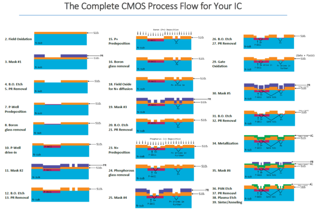 CMOS Process Flow
Current Mask Design for IC Fabrication Course (Spring 2020)
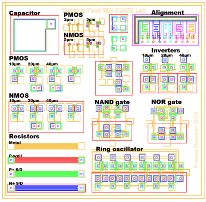 CMOS Mask Layout
(Back to top)