Device Testing Procedure
A common method of indirect evaluation of propagation delay of a CMOS logic circuit is using a ring oscillator. The ring oscillator is constructed simply by chaining an odd number of inverters together and connecting the output of the last inverter to the input of the first. Since this loop has no stable logical output, it oscillates with a period that is a function of the individual inverter delay and the number of inverters (stages) in the loop. The delay through a single inverter stage can therefore be calculated from
τd = 1 / 2nfosc
Where n is the number of stages and fosc is the measured oscillation frequency.
The ring oscillator on an ECE4452 CMOS wafer has five stages and a sixth buffer inverter is shown below. The buffer is necessary to prevent test equipment connected to the output from loading the oscillator loop and thereby changing the period of oscillation. It does not significantly alter the period of oscillation and may be neglected when calculating gate delay.
Once the ring oscillator is connected to the HP6225A Dual Power Supply to power the device on VDD and VSS, and to the Tektronix 1102B Oscilloscope to measure the output (Out), the following procedure may be used to obtain DC characteristic curves:
- Using the HP6225A, set the VDD power supply to 5 V and the VSS supply to 0 V (Ground).
- Turn on the Tektronix 1102B Oscilloscope and set CH1 to using DC mode, the vertical division units to 1 V, the horizontal division units to 50 µs, and the ground level to -2 V.
- Observe the output of the ring oscillator and how it changes if the power supply voltage is varied from 3-5 V. Signal frequency and amplitude can be measured manually or using the oscilloscope measure functions.
Device Testing Setup
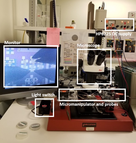 Signatone Probe Station and HP6225A Power Supply
Examples of Testing Results
(Back to top)