When processing, it is a good idea to keep track of how each step looks with different metrology instruments as well as keeping track of the process tool's parameters. This way while processing, trends can be seen which lead to identification of where a process should be stopped, went wrong or what may need to be changed. For micro and nanotechnology, the microstructure can affect a device properties as well as the environment. For example, one time the humidty was above 70% in Petitt and it took a while for users to realize that was the reason why no one's lithography was working that day. This is why now there are sensors which monitor the humdity and you can see it on the active map outside the Petitt cleanroom.
Another good example, one day a user's Cu film started having microcracks and delaminating on a process he had been using for over a year. After a time, it was determine the Cu film's being deposited by the Denton Discovery were at a much higher stress level then before due to the vaccum pump being weaker and leading to higher sputtering pressure and increase in deposition rate.
|
Film thickness measurements are good to ensure the amount of material is deposited, etched or how much a photoresit was developed. Often used in hand with samples to verify rate of deposition or etch on a tool. Some of the tools below may also be used to determine surface roughness. Surface roughness could affect the adhesion of subsequent layers (mechanical interlocking is the mechanisim). See the pro's and con's of the film thickness tools.
|
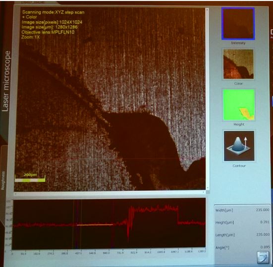
Image: Screen View of the Olympus LEXT 3D Material Confocal Microscope's profilometer of EMC on Cu
|
|
Film uniformity measurements are similar to the thickness measurements in that it ensures the amount of material is deposited uniformally across the whole wafer. Uniformity accross a wafer is important to ensure following processing steps can be done uniformally. May also be used to determine surface roughness. Surface roughness could affect the adhesion of subsequent layers (mechanical interlocking is the mechanisim). See the pro's and con's of the film uniformity tools.
|
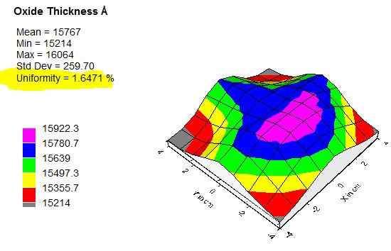 Image: Thickness and Uniformity measurement with Woollam Ellipsometer Oxide Layer deposited by the Plasma Therm PECVD Image: Thickness and Uniformity measurement with Woollam Ellipsometer Oxide Layer deposited by the Plasma Therm PECVD |
|
Often thought of for showing the final MEMS device, taking images along the way can help identify potential issues. Optical microscopes are often used to see if photoresist could be over or under developed. Sems can let users see how large the surface grains are on top, or with the use of cross-sectioning the grains develop through out the structure. Grain sizes can often be related to the electrical, mechanical and thermal performance of a material. Some of the SEMs are equiped with EDX/EDS which allow for potential identification of the alloys at interfaces. See the pro's and con's of the imaging tools.
|
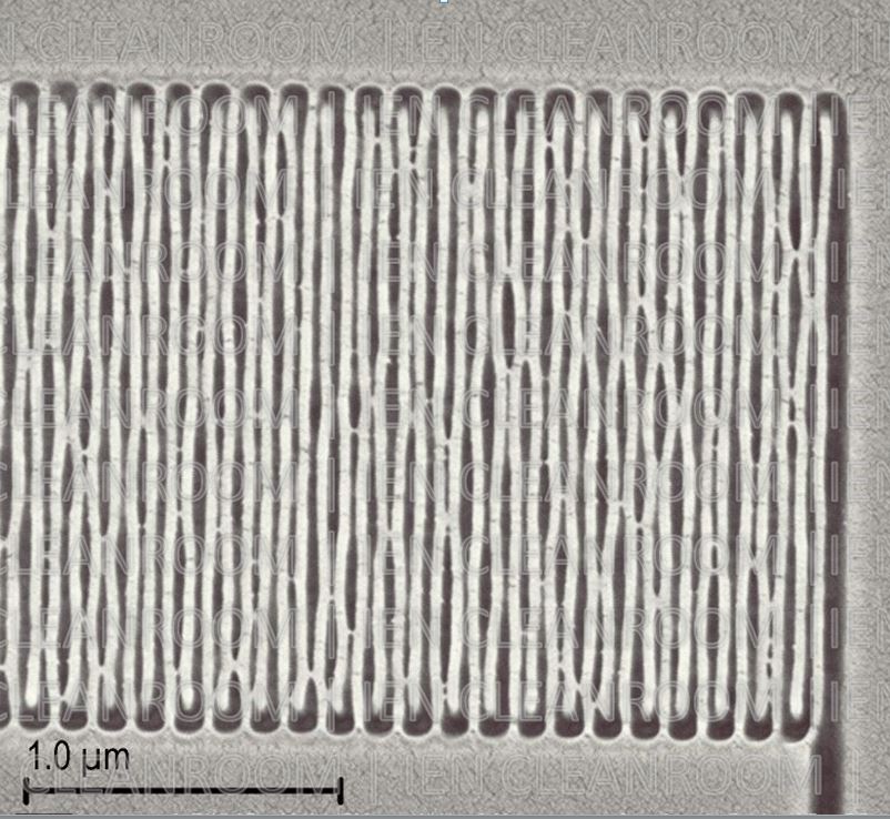
Image: Zeiss Ultra60 FE-SEM image of Resistor (~14nm line spacing) developed by JEOL JBX-9300FS Electron Beam Lithography during a dosage test run.
|
|
Surface properties can be used in various ways. For example, often a quick check to see if a native oxide is removed from a silicon wafer is to run di water over it. Typically (unless specifically treated), di water will bead as it runs across the pure silicon (hydroboic nature) while any silicon oxide would cause the water to hug the surface (hydrophillic nature). The contact angle can be used as a good indicator for if a surface is actually clean. See the pro's and con's of the surface properties tools.
|
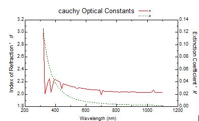
Image: Refractive Index measurement with Woollam Ellipsometer of Oxide Layer deposited by the Plasma Therm PECVD
|
|
Is the low stress nitride really low stress? Check it by utilizing the Bowoptic Stress Measurement. Is the vendor sending the particle distribution claimed? Are there voids forming in the Cu TSVs? Check without destorying the sample in the Dage X-ray. Granted there are resolution limitations. This table list various other metrology tools available in IEN.
|
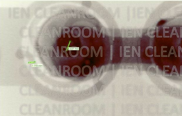
Image: 19 Micron Leg Width Measurements done on a Dage X-Ray XD7600 NT Image of an assembled chip with flexible interconnects (fabricated in the IEN cleanroom) onto an FR 4 Board. (courtasy of S.K. Sitaraman)
|